
Flash Memory Protocol Analysis: eMMC, SD, SDIO, Quad SPI
Flash memory protocol analysis: decoder pages for eMMC, SD 3.0, SDIO 3.0 and Quad SPI, and choosing between LAP-F1 and Bus Expert II.
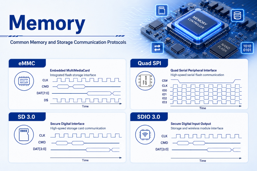
Memory
Flash storage hardware design demands flawless timing margins. This architecture focuses on optimizing data packet and command alignment across eMMC integrated chips, Quad SPI serial flash, and SD/SDIO 3.0 high-speed buses. By integrating advanced hardware measuring methods, we decode bus contention and bit errors during multi-channel read-write cycles, empowering worldwide electronics engineers to verify timing.
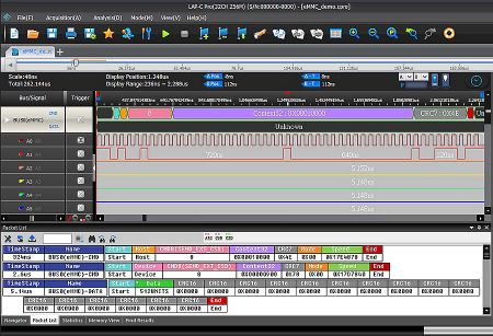
eMMC Protocol Analysis for Memory
eMMC is an embedded memory standard specified by the MMCA and is mainly designed for mobile...
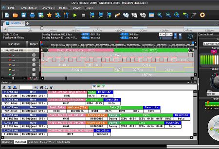
Quad SPI Protocol Analysis for Memory
Quad SPI is mainly applied in EEPROM, FLASH, AD Converter, SPI FLASH in automobile or industry,...
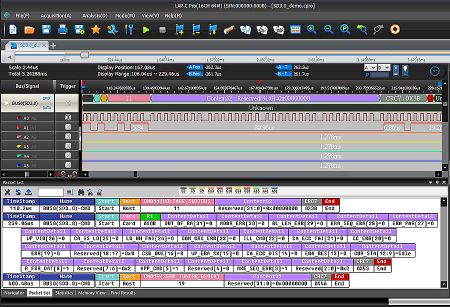
SD 3.0 Protocol Analysis for Memory
SD 3.0 is the next generation of SD 2.0. It is to define higher memory size and higher transmission...
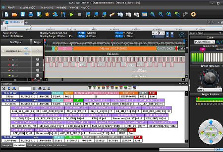
SDIO 3.0 Protocol Analysis for Memory
SDIO 3.0 is a premier interface for mobile and embedded systems, primarily used to connect...
 Download
Popular Products
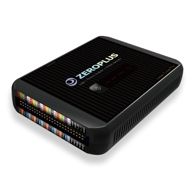
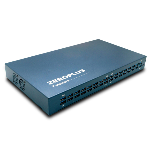
Storage Interface Decoding on LAP-F1 and Bus Expert II
Storage buses combine a command line, a clock and several data lines, and faults usually show up as an unanswered command or a timing violation between them. Zeroplus decoders cover eMMC, SD 3.0 card interfaces, SDIO 3.0 and Quad SPI flash, and eMMC decoding is supported on LAP-F series models and Bus Expert.
Bus Expert II is the dedicated storage instrument, with 32 channels and 2Gb memory depth per channel and support for SD 3.0 and eMMC 4.5, 5.0 and 5.1. On LAP-F1, eMMC 5.1 and SD 3.0 support is an option, which suits projects that also need other buses captured on the same analyzer. For selection, confirm the storage specification version, bus width and clock rate.